Product HighQuality Perfect

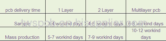
Our deliverytime:
1.About Factory:
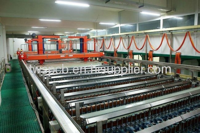
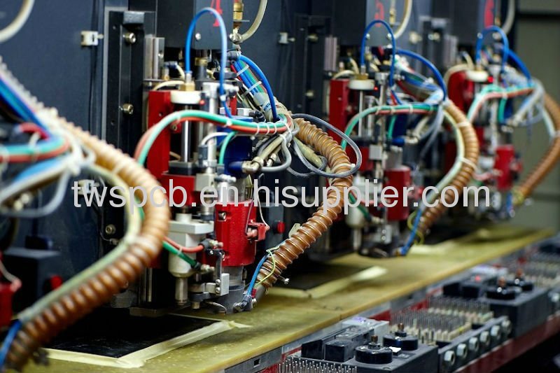
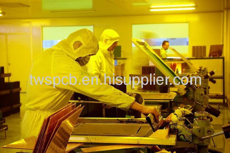
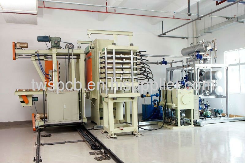
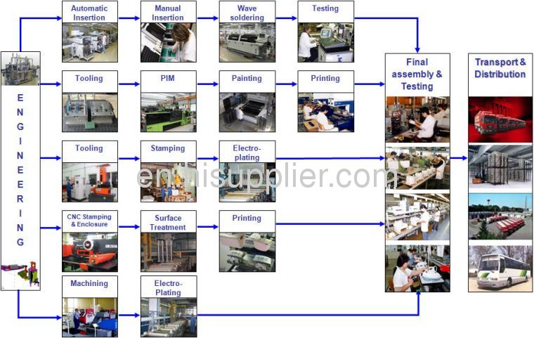
Experience: we have 20 years experinecsin circuit board manufacturing,with 50 employees and 60 excellent engineers,covering an area of 13000 square meters.Monthly capability is more than 5000square meters, 4500 types/month. we cooperate with some well-known enterprises,such as Panasonic, HP,Honeywell and so on.
2.Good after sales service:
anything wrong happening in our products willbe solved within 2 hours. we always offer relative technical support/consultant.Quick response. all your inquiry will be replied within 24 hours.
3.Ourproducts and service are sold well in North America,West Europe, Japan,Singpore, Malaysia and other countries.


Meet your need is ourgreatest pursuit .If you are looking for a pcb board manufacturerinchina,Pleasegive us your files ofpcb for a quote (Gerberfiles and specification),I will reply email in 3hours. Youalso cancontact usby .
1.Advanced production lines andprofessional staff.
2.Honesty credibility in china'stop.
3.Competest price but highquality.
4. One-stopservice.
5.Delivery ontime.

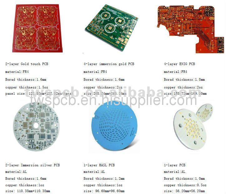
Quick Details
| Place ofOrigin: | Guangdong China (Mainland) | BrandName: | Kingford | ModelNumber: | kingford pcb-809 |
| Number of Layers: | 1 layer | Base Material: | FR4 | Copper Thickness: | 0.5oz |
| Board Thickness: | 1.6mm | Min. Hole Size: | 0.2mm | Min. Line Width: | 2mil |
| Min. Line Spacing: | 2mil | Surface Finishing: | OSP/HAL Lead Free | Color: | Green |
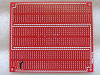
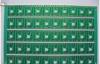
Packaging & Delivery
| Packaging Detail: | Inner packing: vacuum packing/ plastic bag Outer pcaking: standard cartonpacking |
| Delivery Detail: | 1-2 days for sample , 6-14 days for mass production |
Specifications
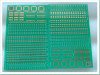
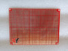
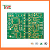
1. FR4material circuit board
2..with UL and ISOcertification
3.Short lead time
4. 100% test before shipment
2..with UL and ISOcertification
3.Short lead time
4. 100% test before shipment
Detail :
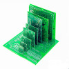
1. Base Material: FR4
2. Layers count: 1 layer
3. SurfaceFinishing :HAL Lead free
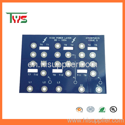
4. Application :LED
What we can do:
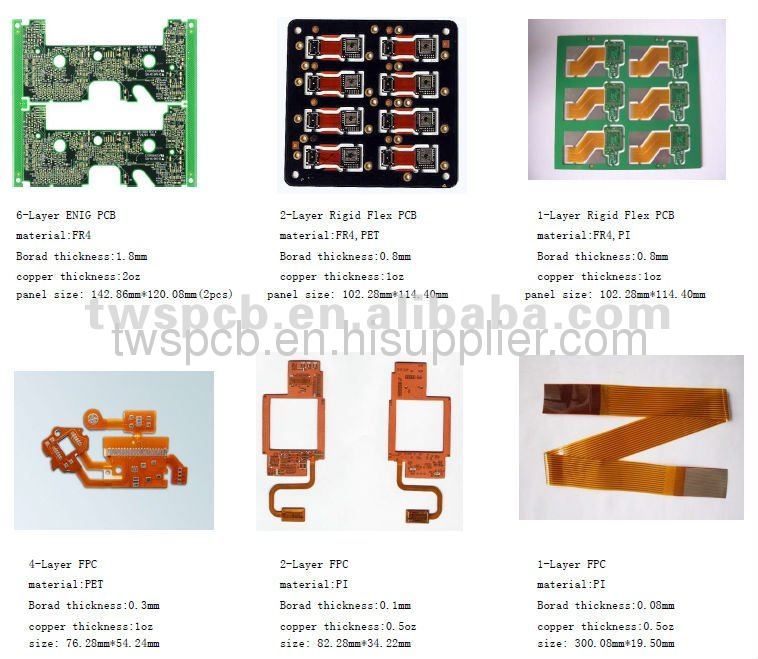
-1 to 30-layer FR-4PCBs with HDI, and metal core PCBs such as Aluminum based PCBs, Copper basedPCBs and Iron based PCBs etc.;
-Production of Prototypes, High-mix, Medium or Low-volume orders with IPCstandards.
Whychoose us:
- Premium services withover 12 years exporting experience;
- Much more competitiveprice than local market in with good quality;
- Short lead time, we cansupport quick turn job too if needed;
- Perfect system (ISO9001-2000, ISO 14001-2004, UL certification, SPC system, etc..)
- Do not haveMOQ
PCBcraft capability
Standard Features | Standard | Advanced |
Maximum layer count | 16 | 32 |
Maximum Panel Size | 21"x24" | 24"x30" |
Outer Layer Trace/Spacing (1/3 oz) | 0.0035"/0.0035" | 0.0025"/0.003" |
[90µm/90µm] | [64µm/76µm] | |
Inner Layer Trace/Spacing (H oz) | 0.003"/0.003" | 0.002"/0.0025" |
[76µm/76µm] | [50µm/64µm] | |
Maximum PCB thickness | 0.125"[3.2mm] | 0.177"[4.5mm] |
Minimum PCB thickness | 0.008"[0.20mm] | 0.004"[0.10mm] |
Minimum mechancial drill size | 0.008"[0.20mm] | 0.004"[0.10mm] |
Maximum PCB aspect ration | 10:01 | 12:01 |
Maximum copper weight | 5 oz [178µm] | 6 oz [214µm] |
Minimum copper weight | 1/3 oz [12µm] | 1/4 oz [9µm] |
Minimum core thickness | 0.002"[50µm] | 0.0015"[38µm] |
Minimum dielectric thickness | 0.0025"[64µm] | 0.0015"[38µm] |
Minimum Pad Size over Drill | 0.018"[0.46mm] | 0.016"[0.4mm] |
Solder Mask Registration | +/- 0.002"[50µm] | +/- 0.0015"[38µm] |
Mimimum Solder Mask Dam | 0.003"[76µm] | 0.0025"[64µm] |
Copper feature to PCB edge | 0.015"[0.38mm] | 0.010"[0.25mm] |
Tolerance on overall dimensions | +/- 0.004"[100µm] | +/- 0.002"[50µm] |
HDI Features | ||
Capture pad size | 0.010"[0.25mm] | 0.009"[0.22mm] |
Glass reinforced dielectrics | Y | Y |
Maximum aspect ratio | 0.6:1 | 1:01 |
Minimum microvia hole size | 0.004"[100µm] | 0.003"[75µm] |
Stacked Microvias | Y | Y |
Copper Filled Microvias | Y | Y |
Maximum No. of buildup layer | 3+N+3 | 4+N+4 |
Quality System and Certificates | ||
IPC-600, 6012, Class II and III | ||
ISO 9001:2008 | ||
UL: E352816 | ||